Schematics
-
After trying to get more information about the AR9331 (the Qualcomm Atheros SoC), I now can imagine at least one reason for not pusblishing the Omega schematics.
It seems that there is no official datasheet and no official pinout available for the AR9331

There are only reverse-engineered pinouts and a probably leaked preliminary datasheet from 2010 on the net.So I suspect the reluctance to publish the hardware could be coming from the legal department. Maybe Onion had to enter a NDA for the AR9331 documentation, and the pinout (which would necessarily be revealed with the schematics) falls under that NDA.
@Lazar-Demin I truly hope I'm not right with this!
-
@Lukas-Zeller said:
And for @onion - I still don't really understand why this is taking so long. You do have the CAD/CAM files - so what's so awfully time consuming? Just print the schematics to PDF from your CAD, and throw them into the HW git repo.
@Lukas-Zeller , when you already now everything better, why the heck you do not start your own IoT project ala "swiss made" and make it better? It is really cheep to sit on a others neck and even accuse them to fooling the customers.
And about the agreement you mentioned in your next request, i think it is also not the right way to find it out this way, posting in the forum your doubt. You better enter in contact with the onioners direct and ask them what they need, resp. how you could help them to resolve the question to publish the "Schematics" as you believe it should be!
This way you just make "bad mood", instead to help to bring the project ahead.
-
@Luciano-S I am sorry you took offense. I don't really understand why, though.
The Onion Omega is a fantastic project as-is, and I am constantly saying that, showing my Omega around and recommending people to buy and use it!
However, it was also announced as an an open hardware project on kickstarter. Of course Kickstarter always bears a risk that promises can't be fulfilled, so I would not blame Onion if going open with the hardware would finally prove too difficult for some reason (I would regret it, very much so).
All I expect is an honest answer. Like a one-liner in this thread saying "look, we underestimated XYZ, and that's why we can't publish the schematics". But it can't be just the time to make that PDF.I definitely do not agree with you that potential IP problems with the AR9331's docs should not be discussed openly. On the contrary, my intention was to raise understanding that there might be external reasons holding the schematics back. I posted it because that information (no published footprint) helps to realize that the situation for Onion might be more difficult than it seemed. IMHO that's the opposite of making "bad mood".
-
@Boken-Lin wow, cooooool! Schematics are in the repo! Thank you very much!
-
@Lukas-Zeller the latest schematics are still the same as pictured here. Is that a careless mistake by Onion team ? Are these schematics reliable ?

-
@Boken-Lin , Could you please also upload the PCB file as the other open source project do ?
-
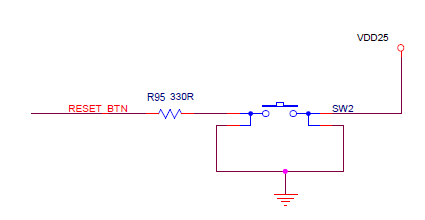
@Ashwani-Mathur As mentioned in a response above: the button schematic object has four terminals, two of them being connected to ground.
The Omega's reset is active-high, so this schematic does make sense, it's just a little confusing. It's important to notice that the blue parts are part of the SW2 schematic object and that they are not actual nets:
- When the button is not depressed, the RESET_BTN net is connected to ground
- When the button is depressed, then the switch closes and the RESET_BTN net gets connected to 2.5V, enabling the reset
So no, not a careless mistake
-
@lazar-demin Dear Lazar, did you see/analyze the drawing??? I will tell you only one as electronic engineer with years of experience: Oh my God! Irrelevant to buttons position (pressed down or not) ACCORDING to the drawing, Resistor R95 right terminal is HELD at GND. The same at VDD25 that YOU FORCED TO GND
Please correct this madness...
-

To clarify the confusion here a bit the component diagram for the button has 4 terminals which maps to the physical switch as shown in the image above. Although it seems that terminals 1,3 or 2,4 are connected they are actually not in the physical button.
-
@Zheng-Han This makes a bit more sense.
However:- I note that the picture of the physical switch actually shows a fifth solder connection - between 1 & 2 in your picture - and I observe that this is soldered on my Expansion Dock
- I still don't understand just how this all works and how the switch is actually connected. @Lazar-Demin above says that the RESET_BTN is connected to ground when the button is NOT depressed. I still don't see how this works given the circuit diagram and your description of the button